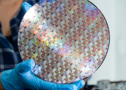
METAPOR® is a high-performance, air-permeable composite material widely used in vacuum clamping applications, particularly in semiconductor manufacturing. Engineered from microporous aluminum or ceramics, METAPOR eliminates the need for drilled vacuum holes while providing uniform suction, high stability, and contamination-free clamping. These properties make it an ideal choice for handling delicate silicon wafers and other sensitive substrates.
Traditional ceramic disk vacuum chucks have been used due to their high precision and rigidity. However, METAPOR line of materials has emerged as a superior alternative to the basic ceramic disc, and offers both a unique microporous aluminum option (BF100 AL) and a superior ceramic based option (CE100), all of which provide enhanced performance at a fraction of the cost. METAPOR can also be used for SMD applications and wire bonding processes.
Overview of Semiconductor Production Stages
Semiconductor manufacturing is a highly complex and precise process, involving multiple stages that transform raw silicon into advanced microchips. At every step, maintaining wafer stability, contamination control, and precision is crucial for achieving high yields and defect-free devices.
- Wafer Fabrication – High-purity silicon is melted and grown into cylindrical ingots, which are then sliced into thin, circular wafers. These wafers are polished to achieve an ultra-smooth, defect-free surface.
- Oxidation & Deposition – Thin insulating and conductive layers are deposited onto the wafer through thermal oxidation, chemical vapor deposition (CVD), or physical vapor deposition (PVD), forming the foundation for transistor structures.
- Photolithography – The wafer is coated with a light-sensitive photoresist, and patterns are transferred onto its surface using UV light exposure through a photomask, defining circuit structures at nanometer scales.
- Etching & Cleaning – Unwanted material is removed using dry (plasma) or wet etching techniques, followed by meticulous cleaning to eliminate residues and contaminants.
- Ion Implantation & Doping – The electrical properties of the silicon wafer are modified by implanting ions to create regions with different conductivity levels, forming the transistor components.
- Interconnect Formation – Multiple metal layers (e.g., copper or aluminum) are deposited and patterned to create interconnections between transistors, forming the chip’s circuitry.
- Testing & Dicing – Once fabrication is complete, wafers undergo a testing process known as Electrical Die Sorting (EDS) to identify functional chips. The wafer is then diced into individual chips.
- Packaging & Final Testing – The diced chips are enclosed in protective packages and tested again before being integrated into electronic devices.
Key Advantages of METAPOR in Semiconductor Vacuum Clamping
- Uniform Vacuum Distribution Without Machined Holes
One of METAPOR’s key advantages is its homogeneous air permeability. Unlike conventional vacuum chucks that rely on drilled suction holes, METAPOR enables:
- Even vacuum distribution across the entire wafer surface, preventing localized pressure points.
- No risk of wafer deformation due to uneven clamping forces.
- Improved handling of ultra-thin wafers, which are prone to warping under traditional clamping systems.
This uniform suction improves the precision and reliability of critical semiconductor processes such as photolithography, etching and wafer processes like polishing, dicing and grinding.
- Contamination-Free Operation
In semiconductor cleanroom environments, contamination is a major concern. Traditional vacuum chucks with drilled holes can trap dust, debris, and process residues, leading to defects in wafers. METAPOR offers a fully sealed, non-porous surface, which:
- Prevents the accumulation of particles that could compromise wafer quality.
- Eliminates the need for filters, reducing maintenance requirements.
- Reduces electrostatic discharge (ESD) risks, ensuring the safe handling of sensitive microelectronics.
This makes METAPOR an ideal solution for applications requiring high-purity wafer processing.
- Non-Damaging, Stable Clamping for Fragile Wafers
As semiconductor technology advances, manufacturers are increasingly working with ultra-thin wafers, compound semiconductors (GaAs, InP), and MEMS devices, which are highly fragile. Conventional vacuum chucks can introduce stress concentrations, leading to cracks or breakage. METAPOR’s microporous structure distributes vacuum evenly, ensuring:
- Gentle, non-contact holding with minimized mechanical stress.
- Edge-free support, reducing the risk of wafer chipping.
- Secure clamping without over-compression, preventing microfractures.
This feature is particularly beneficial for thin wafer handling and backside processing.
- Enhanced Thermal Stability for High-Temperature Processes
Certain semiconductor manufacturing steps, such as etching, deposition, and annealing, involve elevated temperatures. Many conventional vacuum chucks suffer from thermal expansion mismatches, leading to wafer misalignment. METAPOR CE100 provides:
- Low thermal conductivity, dissipating heat efficiently and preventing localized overheating.
- Minimal thermal expansion, maintaining wafer position accuracy during temperature fluctuations.
- Customizable thermal properties, allowing engineers to fine-tune the material for specific semiconductor processes.
This makes METAPOR CE100 particularly effective in plasma etching, lithography, and high-precision laser processing.
-
 Low Maintenance and Long Service Life
Traditional vacuum chucks with drilled suction holes require frequent cleaning and maintenance to remove trapped debris. Over time, these holes can clog, reducing vacuum efficiency and requiring expensive replacements. Basic ceramic disc vacuum chucks can also become brittle and crack. METAPOR’s solid yet air-permeable structure:
- Eliminates clogging, ensuring consistent vacuum performance over long periods.
- Requires minimal maintenance, reducing downtime in production lines.
- Has a durable, wear-resistant surface, prolonging service life compared to conventional ceramic chuck materials.
This translates to lower operating costs and improved manufacturing uptime.
- Aluminum and Non-Aluminum Options
In semiconductor manufacturing, both aluminum and ceramic materials play crucial roles but serve different purposes. Aluminum is primarily used for interconnects and metallization due to its excellent electrical conductivity, ease of deposition, and relatively low cost. However, it suffers from electromigration issues. In contrast, ceramic materials, such as aluminum oxide, silicon nitride, and alumina-based ceramics, are used as substrates, insulators, and packaging materials due to their superior thermal stability, high dielectric strength, and mechanical durability.
It is very important to determine if a project can work with aluminum or not, as some processes do not allow for contact with aluminum. The METAPOR line of materials offers both a unique microporous aluminum option (BF100 AL) and a superior ceramic based option (CE100), to fit every customers need.
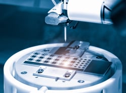
- Compatibility with Automation and High-Throughput Processing
In modern semiconductor fabrication, automation is essential for maintaining high throughput and process efficiency. METAPOR vacuum chucks integrate seamlessly with robotic handling systems, enabling:
- Fast and precise wafer placement and removal for high-speed manufacturing lines.
- Self-centering alignment, improving repeatability and process consistency.
- Versatility for different wafer sizes and materials, including silicon, sapphire, and glass substrates.
This makes METAPOR an excellent choice for automated semiconductor handling solutions.
Switching to METAPOR
METAPOR has revolutionized vacuum clamping by offering uniform vacuum distribution, contamination-free operation, and non-damaging wafer handling. Its thermal stability, low maintenance requirements, and automation compatibility make it a beneficial choice in semiconductor fabrication.
By integrating METAPOR porous ceramic vacuum chucks into lithography, etching, dicing, and inspection processes, semiconductor manufacturers can achieve:
- Lower chuck costs (compared to other ceramic discs)
- Lower maintenance costs
- Easier machinability (regular CNC can be used, no diamond tools or EDM needed)
- Superior flatness
- Low thermal conductivity
- Very low friction and a smooth surface
- Higher wafer yields
- Fewer defects and contamination issues
- Improved process accuracy and repeatability
 The line of METAPOR air-permeable composites are at the forefront of enabling faster, cleaner, and more precise wafer processing, ultimately leading to higher chip yields. Switching to METAPOR’s superior ceramic air-permeable materials, can greatly enhance manufacturing efficiency and product quality in semiconductor manufacturing.